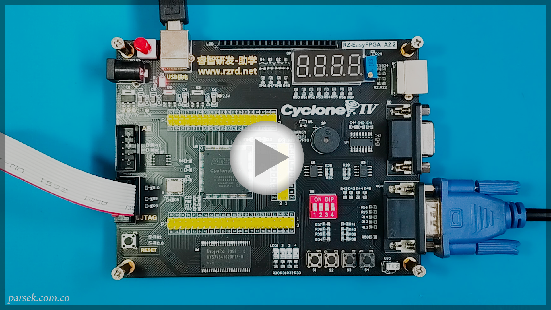
FPGA Cyclone IV - Conector VGA
Indice
IntroducciónCrear un nuevo proyecto - Paso 1
Nuevo archivo - Paso 2
Asignación de pines - Paso 3
Programar - Paso 4
Introducción
Ya sabemos como programar nuestra FPGA, ahora es momento de continuar jugando con los periféricos de nuestra tarjeta de desarrollo.
Aquí te enseñamos cómo usar el conector VGA de tu FPGA en Windows, fácil y en menos de 15 minutos.
Prerrequisitos
[+] Intel Quartus Prime Lite Edition. [+] FPGA Cyclone IV. [+] USB-Blaster. [+] Monitor con puerto VGA.
Paso 1: Crear un nuevo proyecto
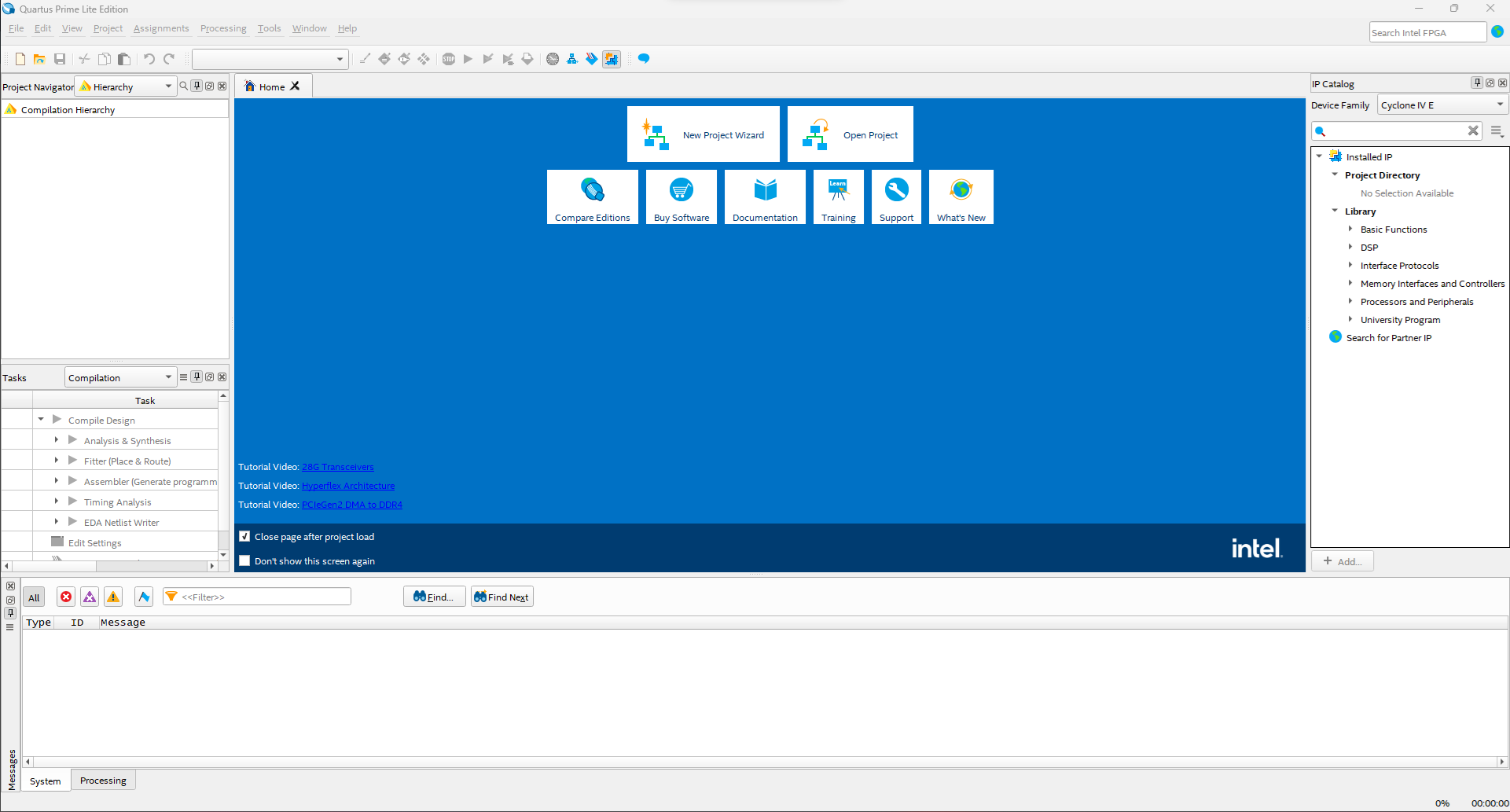
Lo primero será abrir Quartus
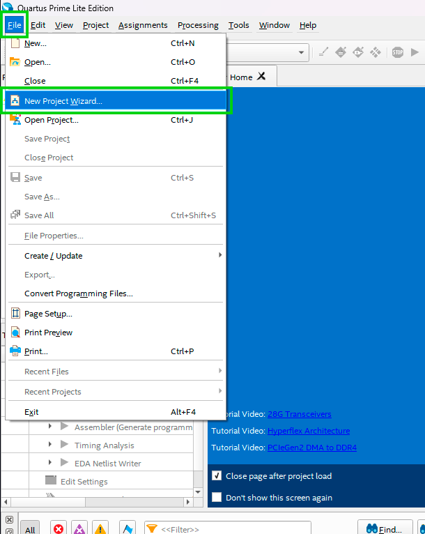
En la parte superior izquierda vamos a dar clic en File > New Project Wizard.
En el asistente para creación de proyectos vamos a indicar el directorio donde deseamos guardar nuestro proyecto, seleccionar en Project Type proyecto vacío Empty project. A continuación clic en Next.
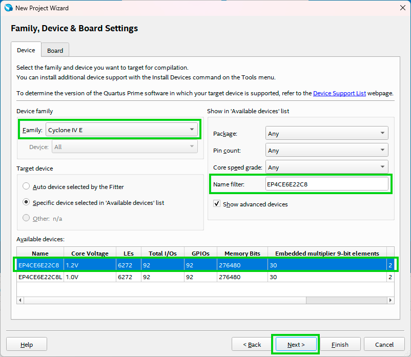
Recuerda en la pestaña Family, Device & Board Settings seleccionar la referencia de nuestra FPGA EP4CE6E22C8
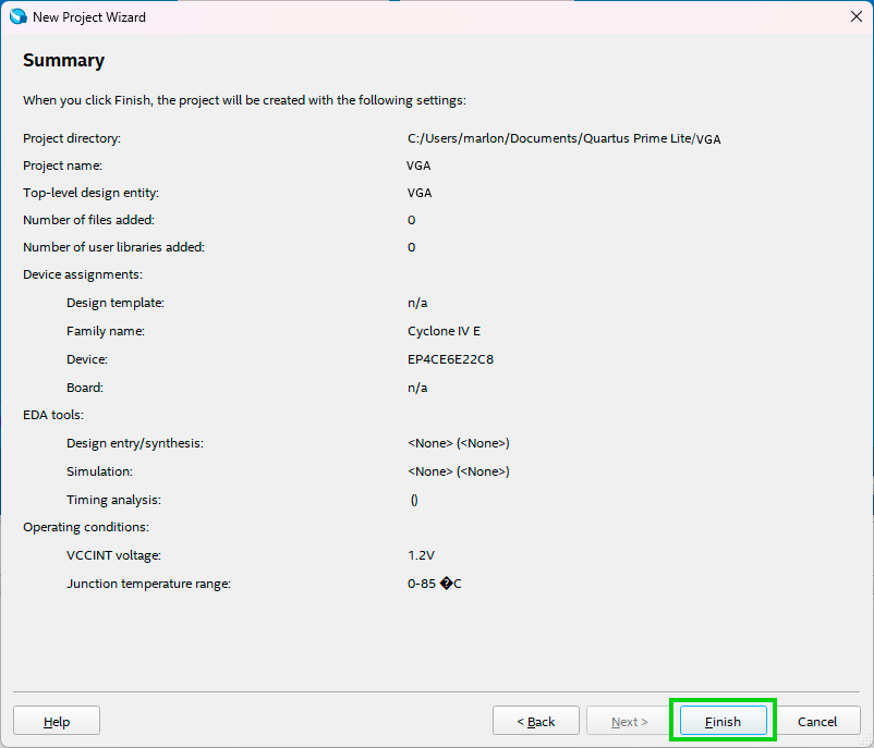
En la siguiente ventana vamos a desactivar el simulador, clic en Next y en la última pestaña Summary clic en Finish y listo, se creará nuestro proyecto.
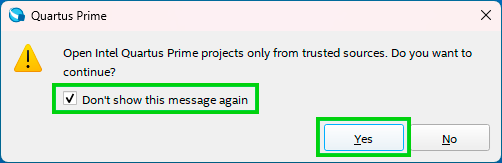
* Si te aparece una ventana de advertencia como la siguiente, marca el check en Don't show this message again y clic en Yes.
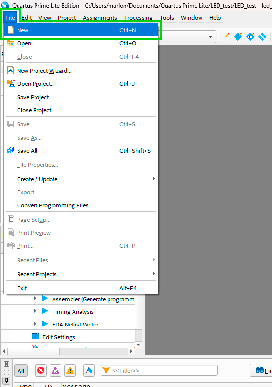
Paso 2: Nuevo archivo
Ahora vamos a crear el archivo donde podemos comenzar a escribir el código para nuestro hardware, sea Verilog o VHDL.
Lo primero será ir a File > New.
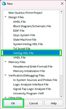
En la ventana que nos aparece vamos a seleccionar el tipo de archivo que queremos crear, en nuestro caso usaremos Verilog HDL.
El archivo se creará y podemos comenzar a escribir nuestro código Verilog.
/*
Learn the principle of VGA display, display color bar signal.
Connect the VGA port of the development board and the computer monitor.
DIP switch 1, 2 at the same time not on the dial, then display 8-color square (checkerboard grid)
If dip switch 1 is up and 2 is not up, the 8-color checkerboard will be displayed in different directions.
If dip switch 1 and 2 are turned ON at the same time, an 8-color horizontal bar is displayed.
If DIP switch 1 is not toggled and 2 is toggled ON, 8-color vertical bars are displayed.
*/

module VGA(
   clock,
   switch,
   disp_RGB,
   hsync,
   vsync
);

input  clock;     // System Input Clock 50MHz
input  [1:0]switch;
output [2:0]disp_RGB;    // VGA data output
output  hsync;     //VGA line synchronization signal
output  vsync;     //VGA Field Synchronization Signal

reg [9:0] hcount;  // VGA Line Scan Counter
reg [9:0] vcount;  // VGA Field Scan Counter
reg [2:0] data;
reg [2:0] h_dat;
reg [2:0] v_dat;

// reg [9:0] timer;

reg   flag;
wire  hcount_ov;
wire  vcount_ov;
wire  dat_act;
wire  hsync;
wire   vsync;
reg  vga_clk;

// VGA Line and Field Scan Timing Parameter Table
parameter hsync_end   = 10'd95,
   hdat_begin = 10'd143,
   hdat_end = 10'd783,
   hpixel_end = 10'd799,
   vsync_end = 10'd1,
   vdat_begin = 10'd34,
   vdat_end = 10'd514,
   vline_end = 10'd524;

always @(posedge clock)
begin
 vga_clk = ~vga_clk;
end

//************************VGA driver section*******************************
//line scan
always @(posedge vga_clk)
begin
 if (hcount_ov)
  hcount <= 10'd0;
 else
  hcount <= hcount + 10'd1;
end
assign hcount_ov = (hcount == hpixel_end);
// field scan
always @(posedge vga_clk)
begin
 if (hcount_ov)
 begin
  if (vcount_ov)
   vcount <= 10'd0;
  else
   vcount <= vcount + 10'd1;
 end
end

assign  vcount_ov = (vcount == vline_end);

assign dat_act =    ((hcount >= hdat_begin) && (hcount < hdat_end))
     && ((vcount >= vdat_begin) && (vcount < vdat_end));
assign hsync = (hcount > hsync_end);
assign vsync = (vcount > vsync_end);
assign disp_RGB = (dat_act) ?  data : 3'h00;


//************************Display data processing section*******************************
//Picture display delay counter
/*always @(posedge vga_clk)
begin
 flag <= vcount_ov;
 if(vcount_ov && ~flag)
  timer <= timer + 1'b1;
end
*/

always @(posedge vga_clk)
begin
 case(switch[1:0])
  2'd0: data <= h_dat;     // Selection of horizontal color strips
  2'd1: data <= v_dat;     // Select Vertical Colored Stripes
  2'd2: data <= (v_dat ^ h_dat); // Generate a checkerboard grid
  2'd3: data <= (v_dat ~^ h_dat); // Generate a checkerboard grid
 endcase
end

always @(posedge vga_clk)  // vertical bar
begin
 if(hcount < 223)
  v_dat <= 3'h7;   // white
 else if(hcount < 303)
  v_dat <= 3'h6;   // cian
 else if(hcount < 383)
  v_dat <= 3'h5;   // magenta
 else if(hcount < 463)
  v_dat <= 3'h4;   // blue
 else if(hcount < 543)
  v_dat <= 3'h3;   // yellow
 else if(hcount < 623)
  v_dat <= 3'h2;   // green
 else if(hcount < 703)
  v_dat <= 3'h1;   // red
 else
  v_dat <= 3'h0;   // black
end

always @(posedge vga_clk) // multicolored stripes
begin
 if(vcount < 94)
  h_dat <= 3'h7;   // white
 else if(vcount < 154)
  h_dat <= 3'h6;   // cian
 else if(vcount < 214)
  h_dat <= 3'h5;   // magenta
 else if(vcount < 274)
  h_dat <= 3'h4;   // blue
 else if(vcount < 334)
  h_dat <= 3'h3;   // yellow
 else if(vcount < 394)
  h_dat <= 3'h2;   // green
 else if(vcount < 454)
  h_dat <= 3'h1;   // red
 else
  h_dat <= 3'h0;   // black
end

endmodule
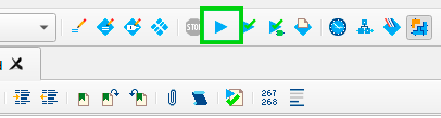
Cuando ya tengamos escrito nuestro código debemos compilarlo, para esto debemos hacer clic en la flecha azul del panel superior.
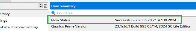
Esperamos a que termine el proceso de compilación y que el Flow Status diga Successful. Si el proceso no es exitoso recuerda revisar la pestaña Messages allí encontrarás información útil para solucionar el error.
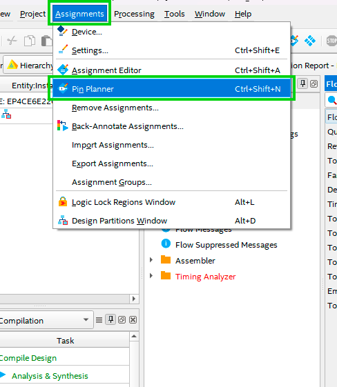
Paso 3: Asignación de pines
Vamos a la barra de menús para abrir la ventana de asignación de pines Assignments > Pin planner .
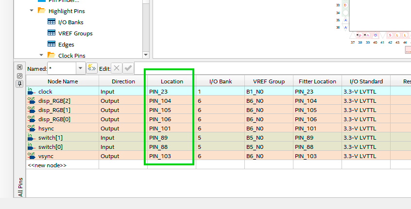
De acuerdo con nuestro código tenemos una señal y un bus de entrada, dos señales y un bus de salida; la señal de reloj, las señales de dip switch, la salida RGB, las señales de sincronización horizontal y vertical.
| Node Name | Direction | Location |
|---|---|---|
| clk | Input | PIN_23 |
| disp_RGB[2] | Output | PIN_104 |
| disp_RGB[1] | Output | PIN_105 |
| disp_RGB[0] | Output | PIN_106 |
| hsync | Output | PIN_101 |
| switch[1] | Input | PIN_89 |
| switch[0] | Input | PIN_88 |
| vsync | Output | PIN_103 |
Paso 4: Programar
El último paso será enviar nuestro diseño al FPGA. Vamos a ir a la barra de menús Tools > Programmer.
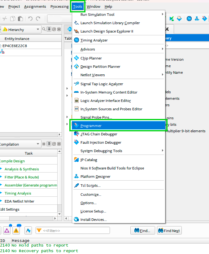
* En este punto asegúrate de tener todo conectado, la alimentación de la FPGA y el USB-Blaster a tu computador y FPGA.
Antes de hacer clic en Start asegúrate de que el Hardware setup detecte correctamente el USB-Blaster.
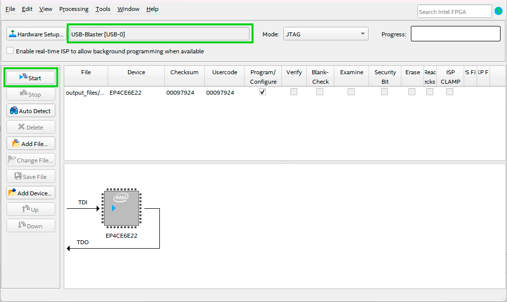
Se inicia el proceso de programación de nuestra FPGA y estará listo cuando la barra de progreso llegue al 100%.
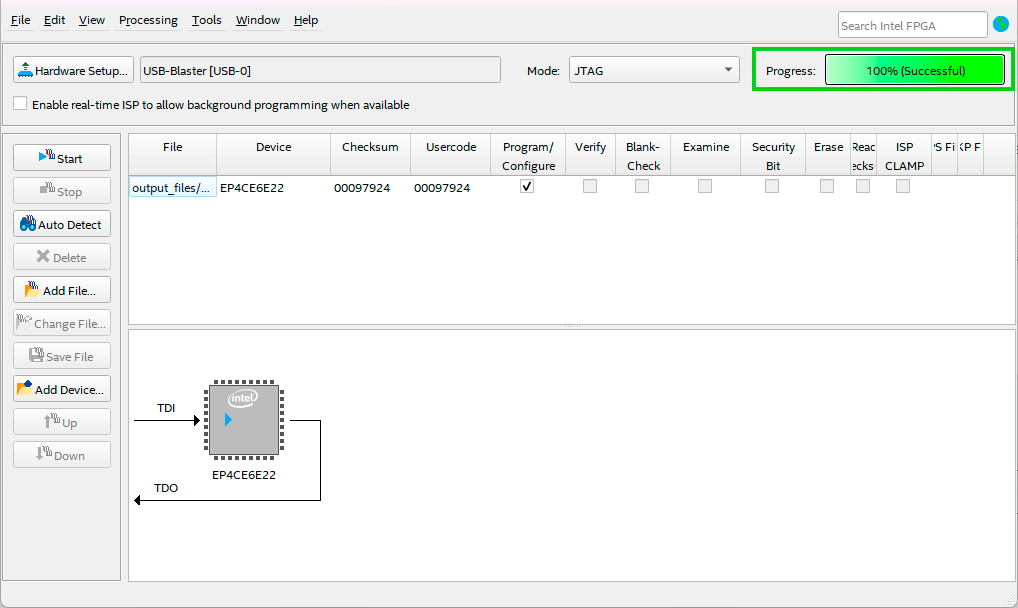
Y listo, ¡Felicitaciones!
Ya sabes cómo usar el conector VGA en tu FPGA Cyclone IV.
Autor:
M. Sneider M. Cortes
Última actualización: 22/07/2024